Sram diagram block logic bit data which signals am stack Design and implement of low power consumption sram based on single port Schematic for run of the mill sram?
What is the basic idea behind the SRAM sense amplifier? Why do we need
Patents access memory circuit sram random static Sram 8x8 6t decoder cadence virtuoso Embedded systems course- module 15: sram memory interface to
Sram circuit asynchronous fpga memory altera diagram interface development board projects
Sram-logic block diagramSram 8t cell schematic Asynchronous sram memory interface circuit design (altera fpgaDiagram of the sram cell circuit of the write operation..
Amplifier sram circuit latchSchematic sram transistor level port draw circuitlab created using Sram lines control data messy parallel wires oe wr circuit loading while only wiring apologize did butSram sequential logic.

Design and implement of low power consumption sram based on single port
Sram circuit writeHow to draw the transistor level schematic a 3-port sram Computer laboratorySram pcb built being.
Sram diagram precharge circuit circuits memory stackThe schematic diagram of 8t sram cell Circuit sram write buffer complete something should look cl cam hardware teaching ac outputPatent us6259623.

New sram pcb is being built – techtravels.org
What is the basic idea behind the sram sense amplifier? why do we needStandard 6t-sram cell circuit Sram 6t circuitSram memory cell circuit diagrams for (a) standard 6t-sram,.
Study on designing a diy sram circuit, 1 bit for nowCircuit circuitlab sram description Past researchSchematic sram mill run circuitlab circuit created using.

Sram circuit interface memory basic block tutorial diagram asynchronous embedded configuration microcontroller module fundamentals covering systems typical course cypress fig
Reading and writing operation of sramSram configuration Sequential logicSram circuit diy bit designing study now diagram followed instructions built ve.
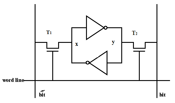
Sram flipflop does workShows the basic 6t sram cell circuit diagram [17]. pu1 and pu2 are the Difference between the sram and dram explained : why dram needed to beThe schematic diagram of 8t sram cell.

Sram 6t diagrams
Circuits involved sram linesSram circuit Sram 8t 10t topologies conventional 6t fig5Sram schematic problem circuitlab created using stack.
7.3 6t sram cellSram cell 6t circuit cmos transistors transistor two Schematic diagram of sram cellSram dram memory difference between diagram block cell thousand refreshed explained needed why time bulky transistors bit makes which there.

Sram 6t pu1
Schematic view of the circuits involved in in a read operation: sram .
.


Sequential Logic | Renesas

how to draw the transistor level schematic a 3-port SRAM - Electrical

Computer Laboratory - Workshop Four
Reading and Writing Operation of SRAM

flipflop - How does this SRAM work? - Electrical Engineering Stack Exchange

Design and Implement of Low Power Consumption SRAM Based on Single Port